 Connect with Google
 Connect with Facebook
Hydroprinting, a Breakthrough Innovation to Print Conductive Patterns.
Posted By Hilmiyati Kusnadi on Jun 28, 2017 | 0 comments
3D printing has been used broadly in the electronics industry for everything that goes around electronic components. In past few years, production of 3D structures with conductive features attracted the attention of many researchers, especially in the field of Internet of Things (IoT). In this blog post, you will discover what researchers have developed despite the difficulties to produce this kind of structures with the regular 3D printing method. Indeed, some researchers finally succeeded in printing conductive patterns using a hydroprinting method.
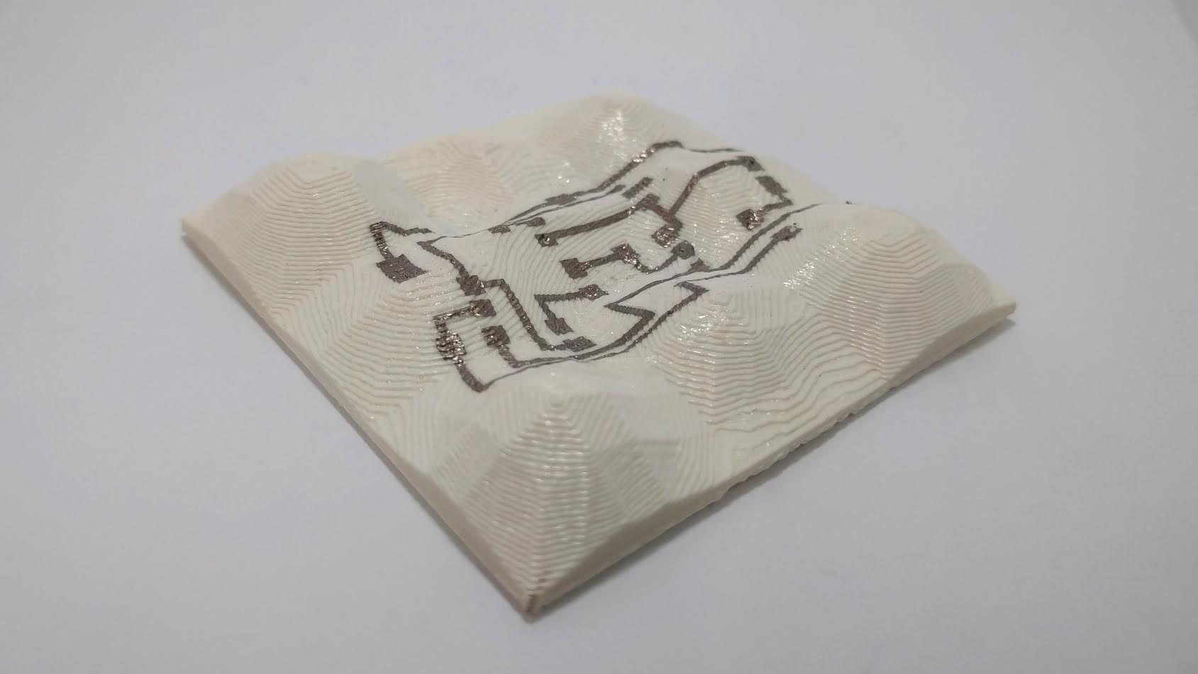
Credits: Dr. Michael Layani
An important challenge due to the complex topography of substrates
When it comes to printing conductive patterns onto a three-dimensional object, the substrates are sometimes uneven and have a very complex topography which makes it difficult to deposit liquids onto the surface.
Also, for the material to be successfully deposited, the substrate has to be placed straight and facing the nozzle and only one material can be printed at a time. Besides the fact that it represents a time-consuming printing process, it often causes the uneven spread of the ink which results in a non-reproducible device.
Hydroprinting, a solution to print conductive patterns
Throughout the recent paper in Advanced Materials Technologies published by Professor Shlomo Magdassi along with some other researchers from The Hebrew University of Jerusalem and The Nanyang Technological University in Singapore, they finally found a solution to the issue mentioned previously.
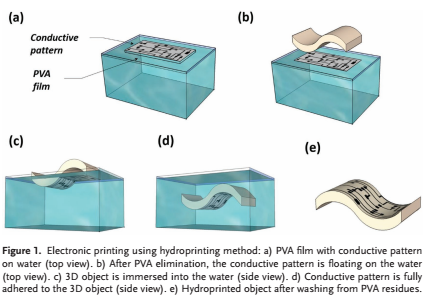
The paper entitled “Hydroprinting Conductive Patterns onto 3D Structures” describes their method to fabricate conductive patterns and circuits using a hydroprinting process. As it is frequently used to print graphic designs for the automotive industry, hydroprinting enables the transfer method to be done efficiently by printing the entire patterns simply in one single step onto a 3D object from all facets.
During the process, polymer is no longer needed and therefore, conductive materials can be placed on top of each other. By adopting this method, printing conductive patterns isn’t a time-consuming process anymore since it only takes minutes to print the patterns.
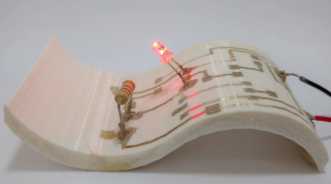
In order to test if this method is a better solution, the researchers conducted an experiment. They hydroprinted a whole optoelectronic 3D device, which was working successfully. According to what Professor Magdassi explained to 3DPrint.com, this breakthrough method is expected to be used for several applications such as fabricating soft robotics parts, 3D electronics, and also for communication devices such as 3D printed Near Field Communication (NFC) antennas.
Credits: Dr. Michael Layani
How does Hydroprinting conductive patterns work
Here is the abstract of the paper “Hydroprinting Conductive Patterns onto 3D Structure”:
“A novel and facile method for printing functional conductive patterns on 3D objects with unconventional angles using hydroprinting of silver nanoparticles (NPs) ink is developed. Silver NPs ink is inkjet printed on water soluble polyvinyl alcohol films. Sintering at room temperature is achieved by exposing the printed pattern to hydrochloric acid fumes. Electric circuits are hydroprinted at low temperature (50 °C) on various 3D-printed structures and materials. The conductive patterns are hydroprinted on hard 90° angle objects and are assembled without any presence of sacrificial layer, which allows layer-by-layer overlap hydroprinting. In addition, electric Light Emmiting Diode (LED) circuits and heater are successfully hydroprinted. To show the applicability of the process we hydroprinted a fully functional Near Field Communication (NFC) antenna onto a curved object, which was successfully paired with a smartphone. Analysis of hydroprinted patterns shows that the resistivity is 17.1 times higher than silver bulk which is considered suitable in most application.”
One last fascinating fact about this new strategy is that it enables to print several layers circuits. It only requires repeating the same printing process for as many layers as needed.
If you wish to learn more about printed electronics and some projects conducted by Professor Shlomo Magdassi, simply follow this page.